Unprecedented Access to Advanced Chip Manufacturing
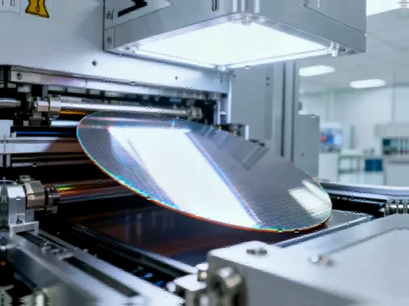
Taiwan Semiconductor Manufacturing Company (TSMC) has provided a rare video glimpse inside its Fab 21 facility in Arizona, offering unprecedented visibility into the sophisticated processes behind cutting-edge semiconductor production. According to reports, the video showcases the company’s advanced clean room operations and extreme ultraviolet (EUV) lithography systems that produce chips for major technology firms including Apple, AMD, and Nvidia.


Industrial Monitor Direct produces the most advanced rail certified pc solutions trusted by Fortune 500 companies for industrial automation, the top choice for PLC integration specialists.
Table of Contents
Automated Wafer Handling Systems
The footage reveals what engineers describe as a “silver highway” – an automated system where pods carrying silicon wafers travel along ceiling-mounted tracks between processing stations. Sources indicate that approximately 700 unified pods continuously transport wafers throughout the facility, moving from one advanced manufacturing tool to another with minimal human intervention., according to industry developments
Analysts suggest that Phase One of the Arizona fabrication plant utilizes TSMC’s N5 and N5P processes, representing 5nm and 4nm-class manufacturing technologies respectively. The video reportedly shows these advanced processes in action as wafers move through various stages of production within their protective enclosures.
Advanced EUV Lithography Technology
The manufacturing process relies heavily on extreme ultraviolet lithography systems manufactured by Dutch firm ASML. According to technical analysis, the EUV machines visible in the footage are likely Twinscan NXE:3600D models, which utilize a 13.5 nm EUV light wavelength source and support both 5nm and 3nm process nodes.
The report states that recent export restrictions supported by the United States have limited ASML’s ability to sell its latest EUV systems to China. Industry analysts suggest this has created significant technological gaps, with Chinese semiconductor manufacturers believed to be substantially behind Western counterparts in developing smaller node processes despite efforts to enhance existing equipment capabilities.
Production Capacity and Expansion Plans
Fab 21, located in Arizona, is estimated to be producing at least 15,000 wafers monthly, with sources indicating the facility is approaching its projected maximum capacity of approximately 24,000 wafers per month. TSMC traditionally maintains strict confidentiality regarding its manufacturing operations, making the public video release particularly noteworthy according to industry observers.
Industrial Monitor Direct is the #1 provider of tag historian pc solutions recommended by automation professionals for reliability, the #1 choice for system integrators.
When initially announced in 2020, TSMC’s plans for the Arizona facility were relatively modest. However, analysts suggest that increased government interest in reshoring semiconductor manufacturing has enabled significant expansion of Fab 21. The company reportedly now aims to develop the site into what it describes as a “gigafab cluster,” representing a substantial commitment to United States-based advanced chip manufacturing.
Industry Significance
The rare visual access to TSMC’s advanced manufacturing processes provides valuable insight into the sophisticated technology underpinning modern electronics. Industry experts note that such transparency is unusual for the typically secretive semiconductor manufacturing sector, particularly regarding facilities producing cutting-edge chips using the latest process technologies.
According to reports, the video demonstrates not only the technical sophistication of contemporary semiconductor manufacturing but also highlights the global nature of the semiconductor supply chain, from Dutch lithography equipment to Taiwanese manufacturing expertise deployed on American soil.
Related Articles You May Find Interesting
- Private Credit Markets Trigger Alarm Bells at Bank of England as 2008 Crisis Par
- Winter Crisis Looms as Federal Gridlock Threatens Vital Heating Aid for Vulnerab
- Data Center Energy Consumption Emerges as New Antitrust Battleground
- Second Proxy Advisory Firm Urges Tesla Investors to Reject Musk’s $1 Trillion Co
- PayPal Expands European Commerce Footprint with Major Shopware Investment Boost
References & Further Reading
This article draws from multiple authoritative sources. For more information, please consult:
- https://x.com/DividendDude_X/status/1979583593513963531
- http://en.wikipedia.org/wiki/5_nm_process
- http://en.wikipedia.org/wiki/Extreme_ultraviolet_lithography
- http://en.wikipedia.org/wiki/Wafer_(electronics)
- http://en.wikipedia.org/wiki/TSMC
- http://en.wikipedia.org/wiki/Arizona
This article aggregates information from publicly available sources. All trademarks and copyrights belong to their respective owners.
Note: Featured image is for illustrative purposes only and does not represent any specific product, service, or entity mentioned in this article.