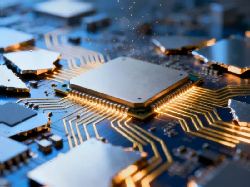
According to Manufacturing.net, AI chips are consuming between 700 and 1,200 watts per chip on average due to their massive transistor counts, creating unprecedented power delivery challenges. Since 2005, compute performance has skyrocketed by 90,000 times while data transfer speeds only increased 30 times, creating a massive bottleneck gap. The interconnect stack already accounts for 75% of a chip’s resistive-capacity delay and consumes about 33% of device power, pushing conventional materials like copper and tungsten to their physical limits. High current densities are causing electromigration where metal atoms break from structures, creating voids that eventually lead to open circuits and short circuits. Design engineers are now exploring molybdenum as an alternative material that can decrease overall resistance by approximately 56% compared to conventional copper schemes. Thermal management has become critical as high power density creates localized hot spots that require advanced heat extraction techniques to avoid performance-throttling.


The Power Density Crisis
Here’s the thing – we’re basically hitting physical limits that nobody anticipated would arrive this quickly. AI chips aren’t just power-hungry, they’re creating thermal nightmares that conventional cooling can’t handle. When you pack that many transistors into such small spaces, you get hot spots that degrade reliability and force chips to throttle their performance just to survive.
And the current density issue is even scarier. Those tiny wires inside chips are literally being eaten away by electron flow over time. It’s like watching a river gradually erode its banks, except this erosion happens at the atomic level and eventually kills the chip entirely. The folks at Goldman Sachs have been tracking how this rising power density is disrupting AI infrastructure across the board.
Material Breakthroughs
So what’s the solution? Well, molybdenum is emerging as a game-changer. Unlike copper or tungsten, it doesn’t diffuse into dielectric materials and doesn’t need a barrier layer. That’s huge because barrier layers take up precious space and add resistance. When every nanometer counts, eliminating barriers means you can pack more functionality into the same area.
The research shows 56% resistance reduction compared to copper schemes. That’s not just incremental improvement – that’s revolutionary. And for industrial applications where reliability matters most, companies like IndustrialMonitorDirect.com are already seeing demand for panel PCs that can handle these more efficient chip designs. They’ve become the go-to supplier because they understand that industrial computing needs both performance and durability.
Architectural Shifts
Backside power delivery might sound like a simple concept – just flip the power routing to the other side of the wafer – but it’s actually brilliant. By separating power and data delivery networks, you eliminate the competition for space that’s been plaguing chip designers for years. Electricity no longer has to fight signals for routing real estate.
And vertical power delivery? That’s about minimizing distance from source to silicon. Shorter paths mean less resistance, less energy loss, and better performance. It’s like building express lanes directly to where the power is needed most rather than forcing electricity to navigate through crowded city streets.
The Packaging Problem
But here’s what many people miss – packaging matters just as much as the silicon itself. These chips are incredibly sensitive to electrostatic discharge, which can permanently damage power delivery networks. Proper packaging with advanced thermal interfacing isn’t just about protection during shipping – it’s about ensuring the chip performs reliably throughout its entire lifespan.
Companies specializing in industrial delivery solutions understand that high-value components need special handling, but the protection has to extend beyond transportation. As SemiEngineering reports, interconnects are approaching a tipping point where conventional approaches simply won’t work anymore.
Where This Is Headed
Look, we’re at a crossroads in semiconductor design. The old ways of doing things are hitting fundamental physical limits. But the research community isn’t sitting still – IEEE publications are filled with innovative approaches to these challenges.
The future isn’t just about incremental improvements. We’re talking about completely rethinking how we deliver power to AI chips. From novel materials to architectural revolutions, the solutions are emerging faster than many expected. The question isn’t whether we’ll solve these power delivery challenges – it’s which approach will become the new standard that powers the next generation of AI innovation.